
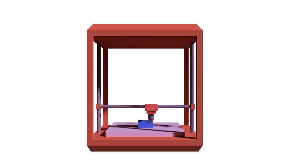
Micro Additive Manufacturing.
Page under construction

Together, initiatives such as Industry 4.0 and the Industrial Internet of Things (IIoT) are helping manufacturing organizations to improve the efficiency of their production processes. Cloud-based analytics applications are responsible for collating and giving context to the many different aspects of running a production or manufacturing operation. These applications harvest the essential data from sensors that are deployed across the factory floor and in every piece of manufacturing equipment. Sensors are used to measure the real-time world, and in most cases, convert the analog measurements into a digital signal. Environmental parameters include temperature, humidity and air pressure, but there are many other characteristics such as gas flow, hydraulic fluid pressure and proximity.
There is are variety of sensors and actuators the major ones being MEMS ( microelectromechanical systems) micro-opto-electro-mechanical systems ( MOEMS) and microelectonic and micro-optical electronics systems (MOES). Also another class of sensors include electrochemical micro sensors.
Microfabrication technoloiges can be categorised correspondingly as MEMS manufacturing and non- MEMS manufacturing methods include laser ablation; photolithograply, electroplating and LIGA, chemical etching etc., Non – MEMS generally include methods like microextrusion, laser patterning/drilling/cutting, microinjection moulding, microstamping etc.

3D Micro Additive Manufacturing
Scalable additive manufacturing
3D Direct writing
Hybrid processes
-
Stereolithography
-
Selective Laser Sintering
-
3D printing
-
Inkjet printing processes
-
Fused Deposition Modelling
-
Laminated Object Manufacturing
Ink-based DW processes
-
Nozzle dispensing: Precision pump and Syringe based methods
-
Aerosol jet
Laser transfer DW:
-
Laser-induced forward transfer (LIFT)
-
Matrix-assisted pulsed laser direct-write (Mapple)
Beam deposition:
-
Laser chemical vapor deposition (LVCD)
-
Focused ion beam DW
-
Electron beam DW
-
Electrochemical Fabrication (EFAB)
-
Shape Deposition Modeling (SDM)

Micro stereo lithography:
Stereo lithography is the first commercial AM process developed by 3D systems inc. which is based on layer-by-layer photosensitive resin polymerization using the Ultra Violet (UV) light.
Micro stereolightography (MSL) is based on conventional stereolithography in which UV laser beam is radiated over the surface of a UV curable liquid polymer. MSL has a submicron resolution and the laser spot has a smaller diameter of a few micrometers, solidification occurs in a very small area of the resin layer by layer enabling microparts with 1-10 micron thickness.
This method is used in various areas such as micro sensors, microfluidic systems, optical waveguides, photonic band gap structures, fluid chips for protein synthesis etc.
Two main MSL techniques have been developed which is differs in the beam delivery system namely scanning MSL and projection MSL. In projection MSL, build time is saved significantly compared with the scanning MSL as the whole layer of photopolymer is cured once via exposure through provided mask
Micro Selective Laser Sintering
Selective laser sintering uses a hight temperature laser to sinter the layers of the fine powders selectively. Available commercial SLS systems are able to produce micro components lager than 500 microns as they have a limited laser focus diameter in between 50 – 300 microns.
The Laser Institute Mittelsachsen e.V. has proposed an innovative approach which was capable of producing components from metals and ceramics with an aspect ratio of upto 12, with a resolution of less than 30 microns and a minimum surface roughness of 1.5 microns. With a 56- mm lens and 1064 nm radiation can be focused onto a spot with a radius 7 μm. A pressure range of 10-3 pa can be maintained by connecting the turbo molecular pump to the build chamber so that different process gases can be utilized during the process. A wide range of metals, including: super alloys,
aluminum (Al), stainless steel, tool steel, cobalt (Co) chromium, and titanium have been processed successfully by micro SLM system.
Three-dimensional printing process
The 3DP process was developed by Massachusetts Institute of Technology and is based on inkjet technology, where the droplets of binder material are deposited over the surface of a powder bed, sticking the powder particles. 3DP has demonstrated the capability to fabricate parts of a variety of materials including ceramics, metals, shape -memory alloys (SMA) and polymers with an array of unique geometries.
Thinner layers and smaller sized particles are required to achieve finer details: micro-scale features. Finer powders have lower surface roughness, thinner layers and promoted printability.
3DP has exhibited fabrication of highly complex and intricate designs and features for micron size metallic parts. Sintering process can be utilized as a post-processing technique to produce high- accuracy micro components, where a special sintering aid is spread as a binder over the powder in the areas which are part cross-section which facilitates fusion more quickly in a sintering furnace.